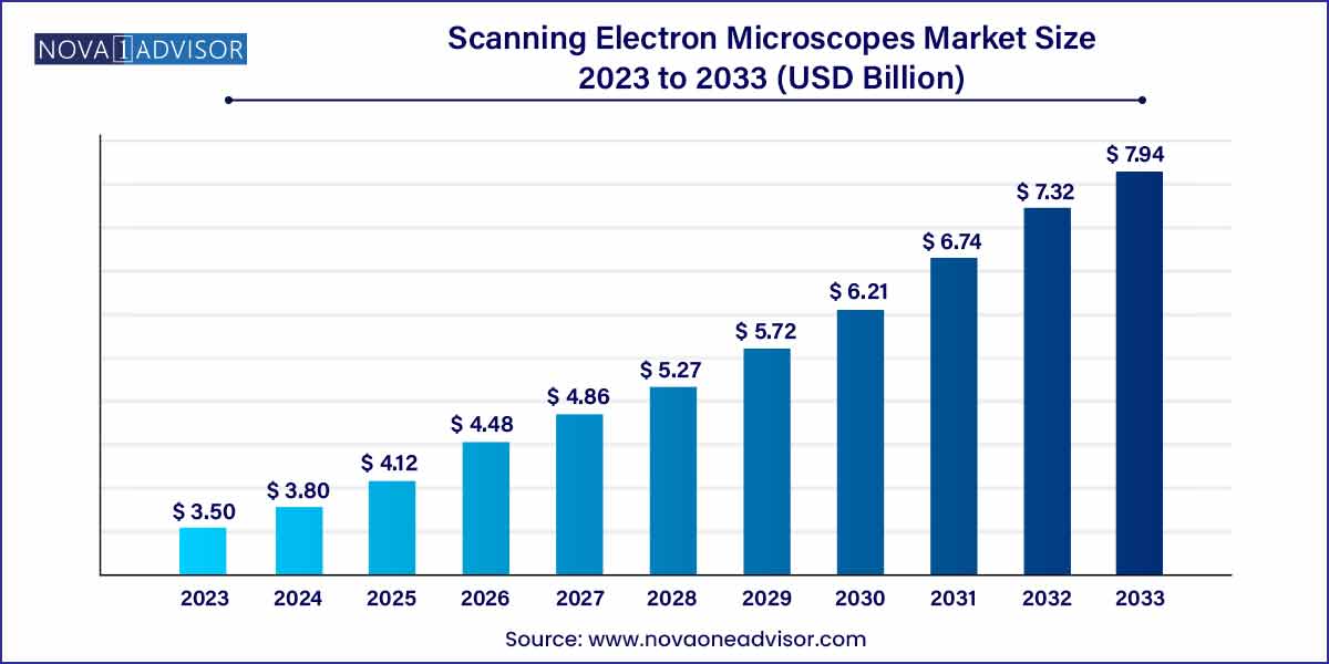
The global scanning electron microscopes market size was estimated at USD 3.50 billion in 2023, is expected to surpass around USD 7.94 billion by 2033, and is poised to grow at a compound annual growth rate (CAGR) of 8.54% during the forecast period of 2024 to 2033.

Key Takeaways:
- The life science segment dominated the overall market with a revenue share of more than 24% in 2023.
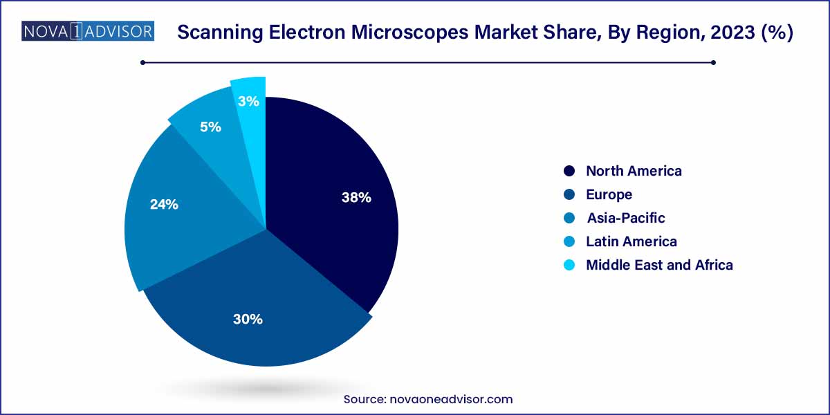
- Asia Pacific held the largest revenue share of more than 38% in 2023.
Market Overview
The global Scanning Electron Microscopes (SEM) Market has established itself as a cornerstone in fields requiring high-resolution imaging and surface characterization at the micro- and nanoscale. SEMs have become indispensable across industries including material science, semiconductor manufacturing, life sciences, and nanotechnology. By utilizing a focused beam of electrons to generate highly detailed images of sample surfaces, SEMs facilitate critical research, product development, and quality assurance processes.
The growing emphasis on miniaturization of electronic devices, advancements in nanotechnology, and rising demand for precision manufacturing are some of the key drivers fueling market growth. Moreover, increasing investments in research and development (R&D) from both academic institutions and industrial sectors have further amplified the need for advanced microscopy techniques.
Technological innovations such as high-throughput imaging, environmental SEMs, and integration of artificial intelligence (AI) for image analysis are redefining SEM capabilities, making these instruments more user-friendly, versatile, and efficient. While cost barriers and operational complexities persist, the expanding application range and improvements in SEM accessibility ensure a promising future for this market.
Major Trends in the Market
-
Adoption of Field Emission Scanning Electron Microscopes (FE-SEM): FE-SEMs are increasingly favored for their superior resolution and image quality.
-
Integration of Artificial Intelligence (AI) and Machine Learning: Automated feature recognition, defect analysis, and pattern detection are becoming standard.
-
Development of Portable and Tabletop SEMs: Compact designs are expanding accessibility to a wider range of users, including educational institutions.
-
Environmental SEMs (E-SEMs) Gaining Traction: Non-destructive imaging of hydrated, biological, and polymeric samples without extensive preparation.
-
Rise in Multi-Detector Systems: Combination of backscattered electron detectors, energy-dispersive X-ray spectroscopy (EDS), and cathodoluminescence detectors for comprehensive analysis.
-
Growing Application in Nanotechnology: As research in nanoparticles, quantum dots, and nanostructures expands, demand for SEMs is intensifying.
-
Increased Focus on User-friendly Interfaces: Simplified software interfaces are enabling less experienced users to operate SEMs efficiently.
-
Strategic Collaborations Between Academia and Industry: Partnerships are driving product innovation and expanding training opportunities.
Scanning Electron Microscopes Market Report Scope
| Report Coverage |
Details |
| Market Size in 2024 |
USD 3.50 Billion |
| Market Size by 2033 |
USD 7.94 Billion |
| Growth Rate From 2024 to 2033 |
CAGR of 8.54% |
| Base Year |
2023 |
| Forecast Period |
2024-2033 |
| Segments Covered |
Applications, Region |
| Market Analysis (Terms Used) |
Value (US$ Million/Billion) or (Volume/Units) |
| Regional Scope |
North America; Europe; Asia Pacific; Central and South America; the Middle East and Africa |
| Key Companies Profiled |
Bruker Corp.; Danish Micro Engineering (DME); Thermo Fisher Scientific; Hitachi High Technologies Corp.; JEOL Ltd.; Leica Microsystems; Nanoscience Instruments, Inc.; Nikon Corp.; Olympus Corp.; Carl Zeiss. |
Driver: Rising Demand in Semiconductor and Electronics Industry
One of the primary drivers propelling the Scanning Electron Microscopes Market is the surging demand from the semiconductor and electronics industries. As device architectures become increasingly intricate with nodes shrinking to below 5 nanometers, manufacturers require ultra-high resolution imaging and precise metrology tools to ensure defect-free production.
SEMs play a pivotal role in semiconductor fabrication processes such as lithography, etching, and failure analysis. Additionally, the adoption of new materials like compound semiconductors and 3D integrated circuits (3D ICs) necessitates advanced surface and structural characterization, further boosting SEM utilization across the sector.
Restraint: High Equipment and Operational Costs
Despite significant technological advancements, the high cost of scanning electron microscopes remains a major restraint for market expansion. SEM systems, particularly high-end FE-SEMs and E-SEMs, involve substantial upfront capital expenditure, often ranging between hundreds of thousands to millions of dollars.
Additionally, operational costs related to maintenance, vacuum systems, consumables, and skilled personnel training add to the financial burden. Small research labs, universities in emerging economies, and smaller industrial players often find it challenging to allocate resources for SEM acquisition and upkeep, limiting broader market penetration.
Opportunity: Expansion of Applications in Life Sciences and Healthcare
A promising opportunity lies in the expanding use of SEMs in the life sciences and healthcare sectors. Modern SEM technologies enable detailed imaging of biological specimens at cellular and sub-cellular levels without the need for extensive sample dehydration.
Applications in pathology, virology, regenerative medicine, and biomaterials research are growing rapidly. For instance, SEM has been instrumental in COVID-19 research for visualizing virus morphology. As interdisciplinary research between biology, medicine, and materials science deepens, SEMs are poised to become integral tools in healthcare innovations.
Application Insights
Material science dominated the SEM market in 2023. SEMs are fundamental to materials research for analyzing microstructures, fracture surfaces, corrosion patterns, and coatings. Universities, metallurgy labs, and industrial R&D centers extensively deploy SEMs for understanding material properties and developing next-generation alloys, composites, and ceramics.
Meanwhile, the nanotechnology segment is expected to experience the fastest growth. With advancements in nanofabrication, drug delivery systems, nanoelectronics, and nanophotonics, precise characterization at nanoscale resolutions is crucial. SEMs, particularly equipped with advanced detectors and automated nanopattern analysis software, are fulfilling these demands, making them indispensable to nanotechnology research.
Additional Application Insights
The life sciences segment is witnessing strong traction, driven by innovations in sample preparation techniques like cryo-SEM, which allow for near-native state imaging of biological specimens. SEMs are increasingly being used for tissue engineering, biomaterials evaluation, and microbiological studies.
In semiconductors, rapid technological shifts toward miniaturized, heterogeneous, and 3D integrated designs are creating a continual need for high-resolution SEM inspection and metrology tools. Consequently, the semiconductor application segment also remains a crucial revenue generator.
Regional Insights
North America led the scanning electron microscopes market in 2023, driven by robust R&D investments, presence of leading universities, strong semiconductor and electronics manufacturing base, and proactive government support for scientific research.
The United States, particularly, boasts major SEM manufacturers like Thermo Fisher Scientific and is home to a network of national labs and research institutes actively engaged in material science, nanotechnology, and life sciences, all of which fuel demand for SEMs. Additionally, collaborations between academia and industries, such as the semiconductor and biotech sectors, strengthen the region's dominance.

Asia-Pacific is projected to register the fastest growth in the coming years. Rapid expansion of the semiconductor manufacturing industry in countries like China, Taiwan, South Korea, and Japan is a major contributor. Furthermore, increasing R&D activities in nanotechnology, material sciences, and biotechnology in these nations are accelerating SEM adoption.
Government initiatives supporting scientific research and manufacturing innovation, coupled with rising investments by global SEM manufacturers to expand their regional presence, are bolstering the Asia-Pacific market. China’s "Made in China 2025" initiative and Japan’s focus on advanced materials research are particularly noteworthy drivers.
Recent Developments
-
March 2025: Thermo Fisher Scientific launched the "Apreo 2 SEM," featuring enhanced automation and AI-driven image analysis capabilities for faster defect inspection in semiconductor manufacturing.
-
January 2025: Hitachi High-Tech Corporation unveiled its latest Tabletop SEM (TM4000 Plus II), offering improved resolution and energy-dispersive X-ray spectroscopy (EDS) integration for educational and industrial users.
-
December 2024: JEOL Ltd. announced the development of the "JSM-IT710HR," an analytical SEM with superior performance for nanomaterials and thin film analysis.
-
October 2024: Carl Zeiss AG introduced "ZEISS GeminiSEM 560," designed for high-resolution surface imaging with automated workflow solutions aimed at material sciences and life sciences applications.
-
August 2024: TESCAN ORSAY HOLDING launched its "TESCAN Clara SEM," featuring a modular architecture and in-situ capabilities for environmental and dynamic sample studies.
Some of the prominent players in the scanning electron microscope market include:
- Bruker Corp.
- Danish Micro Engineering (DME)
- Thermo Fisher Scientific
- Hitachi High Technologies Corp.
- JEOL Ltd.
- Leica Microsystems
- Nanoscience Instruments, Inc.
- Nikon Corp.
- Olympus Corp.
- Carl Zeiss
Segments Covered in the Report
This report forecasts revenue growth at global, regional, and country levels and provides an analysis of the latest industry trends in each of the sub-segments from 2021 to 2033. For this study, Nova one advisor, Inc. has segmented the global scanning electron microscope market.
Applications
- Material Science
- Nanotechnology
- Life Science
- Semiconductors
- Other Applications
By Region
- North America
- Europe
- Asia-Pacific
- Latin America
- Middle East & Africa (MEA)


